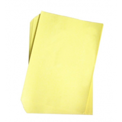
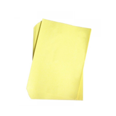
Pelicula Film Fotosensible 30cm X 5 Metros Fabricacion Pcb Fotopolimero Itytarg
10204
Nuevo producto
Este producto ya no está disponible
Más
IMPORTANTE - LEA ATENTAMENTE ANTES DE COMPRAR
ESTE PRODUCTO REQUIERE DE EXPERIENCIA PARA OBTENER RESULTADOS SATISFACTORIOS
EL PRECIO NO INCLUYE LOS QUIMICOS REVELADORES
NO COMPRE EL PRODUCTO SI NO CONOCE SU USO
NO BRINDAMOS ASESORAMIENTO SOBRE ESTE PRODUCTO
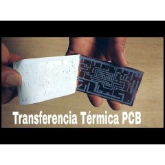
FILM FOTOSENSIBLE PARA CIRCUITOS IMPRESOS
Material foto-polímero resistente a los químicos
para grabado de circuitos impresos
Capaz de reproducir fielmente el patrón del circuito
con luz ultra violeta a través de un negativo.
Es posible obtener resultados profesionales en
montaje superficial.
Resultado 100% profesional
VENTAJAS Y ESPECIFICACIONES
Color................................................: azul
Espesor ...........................................:40 micrones
Rango de Exposición.......................:365 a 400 nm
Química ............................................:negativa
Resolución.........................................:0,06 mm
Revelado............................................Solución
Almacenaje:........................................5-21 C, 30-70% HR
Alta definición en la formación de imágenes
Gran adherencia a diversos materiales
Revelado y eliminación fácil y segura ( no tóxico)
Excelente costo beneficio
Condition: New: A brand-new, unused, unopened, undamaged item in its original packaging (where packaging is applicable). Packaging should be the same as what is found in a retail store, unless the item is handmade or was packaged by the manufacturer in non-retail packaging, such as an unprinted box or plastic bag. See the seller's listing for full details. See all condition definitions- opens in a new window or tab ... Read moreabout the condition
30cm Photosensitive Dry Film Replace Thermal Transfer PCB Board Longth 5M
Feature:
Width: 30cm
Length: 5M
1.5 mil thickness of dry film can be completely cover a hole of 0.25 inches
The dry film can be used in the most ordinary plating solution, no wrinkle, no discoloration
Operating steps:
1, grinding CCL,using the finest polished clean water frosted paper on the line.
2, removing film, photographic film is sandwiched between two layers of film, the first side can make use of transparent tape tear torn, try a few on the line.
3, and then foil, copper clad laminates can look a little cleaner, pasted, try not to have bubbles.
4, good paste membrane used presses, not too hot, about 100 degrees from the fixing.
5, the printed circuit board film, suggestion is to use film, the fine could reach the highest degree of accuracy if you did not ask for the paper to print it with sulfuric acid trip.
6, the printed circuit on the photographic plate (Note: Dry film is negative, so to highlight the print, which we usually use photographic plate opposite) with ordinary energy-saving lamps 10 or so, if there is exposure Machine 1 minutes on the line, the sun not tried, it should be 30 seconds -60 seconds, the exposure process Obviously, since the photosensitive film will change color when exposed to light, the light becomes dark blue. You will easily see your circuit diagram appeared on the board.
7, developing and tear the protective film on the front panel, into the developer (developer according 1:100,10 g Total 1L of water) to be used when developing a little harder stick cotton wipe board.
8, etching, this goes without saying (ferric chloride etchant environmental protection, hydrochloric acid + hydrogen peroxide, etc.) is recommended environmental etching shop, fast, clean, no odor.
9, after a good CCL etching, stripping, from film watered by 1:60 or 70, the board bubble like a few minutes,
10, after the completion of the board, very pretty good, most dense line spacing is 0.1MM, width 0.1MM, 0.1
Ejemplo de uso
3 productos más en la misma categoría:
-

Mejor Precio Garantizado
En nuestra tienda encontrará los mejores precios.
-

Soporte
Por cualquier duda, puede comunicarse con nosotros.
-

Ofertas
Acceda a las mejores ofertas en nuestros productos.