Ver más grande

¡Disponible sólo en Internet!
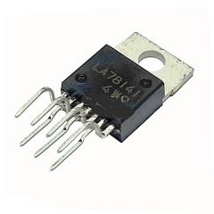
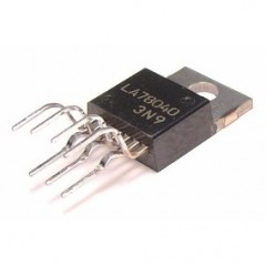
Tda3653b Tv Deflexion Vertical Itytarg
MLA637077742
Nuevo producto
7 artículos
Más
GENERAL DESCRIPTION
The TDA3653B/C is a vertical deflection output circuit for drive of various deflection systems with currents up to
1.5 A peak-to-peak.
Features
• Driver
• Output stage
• Thermal protection and output stage protection
• Flyback generator
• Voltage stabilizer
• Guard circuit
FUNCTIONAL DESCRIPTION
Output stage and protection circuit
Pin 5 is the output pin. The supply for the output stage is fed to pin 6 and the output stage ground is connected to pin 4.
The output transistors of the class-B output stage can each deliver 0.75 A maximum.
The maximum voltage for pin 5 and 6 is 60 V.
The output power transistors are protected such that their operation remains within the SOAR area. This is achieved by
the co-operation of the thermal protection circuit, the current-voltage detector, the short-circuit protection and the special
measures in the internal circuit layout.
Driver and switching circuit
Pin 1 is the input for the driver of the output stage. The signal at pin 1 is also applied via external resistors to pin 3 which
is the input of a switching circuit. When the flyback starts, this switching circuit rapidly turns off the lower output stage
and so limits the turn-off dissipation. It also allows a quick start of the flyback generator.
External connection of pin 1 to pin 3 allows for applications in which the pins are driven separately.
Flyback generator
During scan the capacitor connected between pins 6 and 8 is charged to a level which is dependent on the value of the
resistor at pin 8 (see Fig.1).
When the flyback starts and the voltage at the output pin (pin 5) exceeds the supply voltage, the flyback generator is
activated.
The supply voltage is then connected in series, via pin 8, with the voltage across the capacitor during the flyback period.
This implies that during scan the supply voltage can be reduced to the required scan voltage plus saturation voltage of
the output transistors.
The amplitude of the flyback voltage can be chosen by changing the value of the external resistor at pin 8.
It should be noted that the application is chosen such that the lowest voltage at pin 8 is > 2.5 V, during normal operation.
Guard circuit
When there is no deflection current and the flyback generator is not activated, the voltage at pin 8 reduces to less than
1.8 V. The guard circuit will then produce a DC voltage at pin 7, which can be used to blank the picture tube and thus
prevent screen damage.
Voltage stabilizer
The internal voltage stabilizer provides a stabilized supply of 6 V to drive the output stage, which prevents the drive
current of the output stage being affected by supply voltage variations.
3 productos más en la misma categoría:
-

Mejor Precio Garantizado
En nuestra tienda encontrará los mejores precios.
-

Soporte
Por cualquier duda, puede comunicarse con nosotros.
-

Ofertas
Acceda a las mejores ofertas en nuestros productos.