Ver más grande

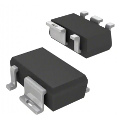
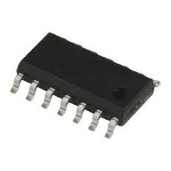
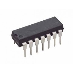
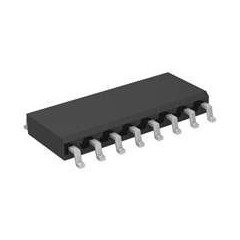
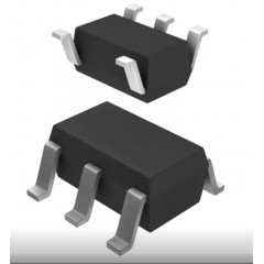
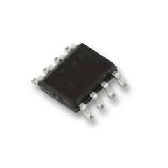
Cd4066 Llave X 4 Switch Cmos Smd Soic14 Itytarg
MLA664788657
Nuevo producto
Cod: KDY
Origen: USA
TIPO: CD4066BM96G4
100 artículos
Más
CD4066 es un circuito integrado de la familia CMOS (semiconductor complementario de óxido metálico) que posee en su interior 4 interruptores bilaterales, los cuales son controlados digitalmente por 4 terminales de control, cada uno con controles independientes. El CD4066 puede manejar señales analógicas y digitales, además es compatible con el CD4016 pero se diferencia en que sus interruptores poseen una menor resistencia. La operación del CD4066 es muy simple, tenemos 4 interruptores bilaterales, esto quiere decir que no importa si colocamos la señal a la entrada o a la salida, el resultado siempre será el mismo.
Por otro lado tenemos los terminales de control, uno por cada interruptor, lo que obviamente nos da 4 terminales de control. Cada terminal de control del CD4066 es activo en alto. Esto significa que si tenemos un estado alto (voltaje cercano o igual al VCC del CD4066) el interruptor correspondiente se activara y dará paso a la señal que esta conectada a el.
Cuando el terminal de control regrese al estado bajo (voltaje cercano a 0 en el CD4066), el interruptor se colocara en estado de alta impedancia(resistencia muy alta o infinita) con lo cual la señal que es objeto de conmutación, no pasara a través del circuito. Para entender más claramente el funcionamiento del CD4066, observemos la imagen de la tabla de la verdad.

Principales características
Puede conmutar, multiplexar señales analógicas y digitales.
Soporta el conmutado de señales de hasta 20v.
Maneja señales de hasta 40Mhz.
Temperatura de operación: -65ºC a +125ºC
Voltaje de operación típico: 3.3 Vcc a 18 Vcc
Tecnología: CMOS
Fabricantes: Texas instruments (CD4066BE), Philips HEF4066B, Intersil (CD4066).
Aplicaciones
El CD4066 es un interruptor bilateral cuadrático destinado a la transmisión o la multiplexación de señales analógicas y digitales.
1 Features
1• 15-V Digital or ±7.5-V Peak-to-Peak Switching
• 125-Ω Typical On-State Resistance for
15-V Operation
• Switch On-State Resistance Matched to Within
5 Ω Over 15-V Signal-Input Range
• On-State Resistance Flat Over Full
Peak-to-Peak Signal Range
• High ON/OFF Output-Voltage Ratio:
80 dB Typical at fis = 10 kHz, RL = 1 kΩ
• High Degree of Linearity: <0.5% Distortion Typical
at fis = 1 kHz, Vis = 5 Vp-p
VDD – VSS ≥ 10 V, RL = 10 kΩ
• Extremely Low Off-State Switch Leakage,
Resulting in Very Low Offset Current and High
Effective Off-State Resistance: 10 pA Typical at
VDD – VSS = 10 V, TA = 25°C
• Extremely High Control Input Impedance
(Control Circuit Isolated From Signal Circuit):
1012 Ω Typical
• Low Crosstalk Between Switches: –50 dB Typical
at fis = 8 MHz, RL = 1 kΩ
• Matched Control-Input to Signal-Output
Capacitance: Reduces Output Signal Transients
• Frequency Response,
Switch On = 40 MHz Typical
• 100% Tested for Quiescent Current at 20 V
• 5-V, 10-V, and 15-V Parametric Ratings
2 Applications
• Analog Signal Switching/Multiplexing: Signal
Gating, Modulators, Squelch Controls,
Demodulators, Choppers, Commutating Switches
• Digital Signal Switching/Multiplexing
• Transmission-Gate Logic Implementation
• Analog-to-Digital and Digital-to-Analog
Conversions
• Digital Control of Frequency, Impedance, Phase,
and Analog-Signal Gain
Description
The CD4066B device is a quad bilateral switch
intended for the transmission or multiplexing of
analog or digital signals. It is pin-for-pin compatible
with the CD4016B device, but exhibits a much lower
on-state resistance. In addition, the on-state
resistance is relatively constant over the full signalinput range.
The CD4066B device consists of four bilateral
switches, each with independent controls. Both the p
and the n devices in a given switch are biased on or
off simultaneously by the control signal. As shown in
Figure 17, the well of the n-channel device on each
switch is tied to either the input (when the switch is
on) or to VSS (when the switch is off). This
configuration eliminates the variation of the switchtransistor threshold voltage with input signal and,
thus, keeps the on-state resistance low over the full
operating-signal range.
The advantages over single-channel switches include
peak input-signal voltage swings equal to the full
supply voltage and more constant on-state
impedance over the input-signal range. However, for
sample-and-hold applications, the CD4016B device is
recommended.
23 productos más en la misma categoría:
-
Bts3800slhtsa1 Llave Power...
-

4066 Llave Bilateral X 4 Switch...
-
Lote 5 X 4066 Llave Bilateral X...
-

Lote 5 X Cd4066 Llave Cuadruple...
-
Tps2062 Switch Llave Mosfet...
-
Cd4066 4066 Llave Bilateral X 4...
-

Cd4016 4016 Llave Bilateral...
-
Ap2281-3wg-7 Load Switch Llave...
-
Mic2026-1ym High Side Mosfet...
-
Bts740s2 Power Switch Mosfet...
-
Switch Cuadruple Adg433brz Spst...
-
Power Switch Mosfet Bts740s2...
-
Llave Mosfet Multiple Octal...
-
Analogico Switch Cmos Dg418 Spst...
-
Switch High Side Power Mosfet...
-

Switch Mosfet N Bts6143 38v 41a...
-
Switch Mosfet Chn Bts462 38v...
-
Switch Power Mosfet Bts6143...
-
Switch Mosfet Chn Bts426 38v...
-
Switch Mosfet Ap2191 Chp 1:1...
-

Power Switch High Side...
-
Power Switch Auips7091 High Side...
-

Analogico Switch Cmos Ts12a4514d...
-

Mejor Precio Garantizado
En nuestra tienda encontrará los mejores precios.
-

Soporte
Por cualquier duda, puede comunicarse con nosotros.
-

Ofertas
Acceda a las mejores ofertas en nuestros productos.