Ver más grande


¡Disponible sólo en Internet!
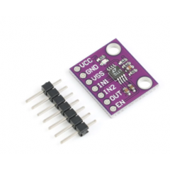
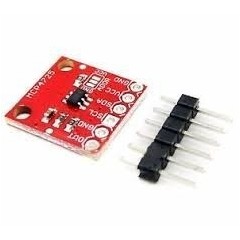
Interfaz Conversor A/d D/a Pcf8591 I2c Itytarg
MLA681957394
Nuevo producto
Cod: HJG-B156
DAC/ADC
7 artículos
Más
Voltaje de funcionamiento: 2.5-6V
A través de la entrada / salida en serie del bus I2C
PCF8591 por 3 direcciones de direccionamiento de hardware
Tasa de muestreo PCF8591 I2C bus rate decided
4 entradas analógicas programables como entradas unipolares o diferenciales
Selección automática de canales incrementales
PCF8591 rango de voltaje analógico de VSS a VDD
PCF8591 circuito integrado de seguimiento y retención
Conversor A / D de aproximación sucesiva de 8 bits
A través de una ganancia DAC de salida analógica
Chip: PCF8951
Tamaño: los 3.6cm * 2.3cm
El PCF8591 es un conversor analógico a digital y digital a analógico de 8 bits de resolución que se comunica con el microcontrolador por medio del bus I2C.
Este componente puede ser útil básicamente en tres líneas de aplicación:
- Añadir una salida analógica, funcionalidad que no está presente en un microcontrolador convencional. El PCF8591 ofrece una salida analógica de 8 bits.
- Aumentar el número de entradas analógicas disponibles. El PCF8591 dispone de cuatro entradas analógicas de 8 bits.
- Incrementar la distancia entre los sensores analógicos y el microcontrolador sin perder o distorsionar la señal. Como el PCF8591 convierte en digital la señal medida y la transmite por I2C, el riesgo de interferencias o pérdida de señal disminuye lo máximo posible a la vez que es posible usar tanta distancia (longitud de cable) como permita el bus I2C
Aunque su resolución de 8 bits es modesta, puede servir para muchas aplicaciones y su precio y su sencillez de uso tanto a nivel de programación como a nivel electrónico lo han hecho muy popular. Como además está disponible en formato DIP es perfecto para pruebas y prototipos.
Para hacer más cómodas las pruebas existen en el mercado módulos que integran el PCF8591 y algunos sensores sencillos (luz y temperatura, normalmente) además de resistencias variables con las que establecer valores analógicos arbitrarios.
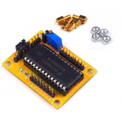
PCF8591 AD/DA Analog-Digital-Analog Converter Module
Description
Key indicators:
Single-Supply Operation
PCF8591 operating voltage range of 2.5V to 6V
Low standby current
through the I2C bus serial input / output
PCF8591 by 3 hardware address pins addressing
Sampling rate PCF8591 I2C bus rate decided
4 analog inputs programmable as single-ended or differential inputs
Automatic incremental channel selection
PCF8591 analog voltage range from VSS to VDD
PCF8591 built-in track and hold circuit
8-bit successive approximation A / D converter
through an analog output DAC gain
Discription:
1. A module chip using PCF8951
2. module supports external voltage input capture (input voltage range 0-5v)
3. Three modules integrated photoresistor acquisition environment through the AD intensity accurate numerical
4. modules integrated thermistor, can capture the precise value of the ambient temperature through the AD
5. The five-module integrated 1 channel 0-5V voltage input acquisition (blue potentiometer to adjust the input voltage)
6. modules with power indicator light (on the module after power indicator lights)
7. modules with the DA output indicator light board DA output indicator module DA output interface voltage reaches a certain value, the voltage the greater the light brightness is more obvious;
8. module PCB size: 3.6cm * 2.3cm
9. standard double-sided, plate thickness 1.6mm, the layout is nice, surrounded by the through-hole, aperture: 3mm, convenient fixed
Interface:
The module's left and right, respectively, the external expansion of 2-way pin interface, respectively, as follows:
Output interface of the left the AOUT chip DA
The AINO chip analog input interface.
AIN1 chip analog input interface
AIN2 chip analog input interface
AIN3 chip analog input interface
The right side of the SCL IIC clock interface to access the microcontroller IO port
The SDA IIC digital interface connected microcontroller IO port
GND module to an external
VCC power supply interface external 3.3v-5v
Module red jumper instructions for use
Module three red short circuit cap, respectively, the role are as follows:
P4 connected to the P4 jumper, select thermistor access circuit
P5 connected to P5 jumper to select the photoresistor access circuit
P6 connected to the P6 jumper, to select 0-5V adjustable voltage access circuit
22 productos más en la misma categoría:
-
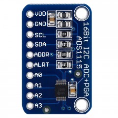
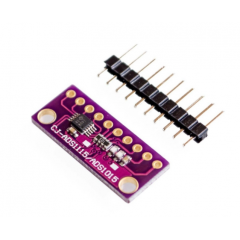
Pga Ads1115 16bit Adc - 4ch...
-
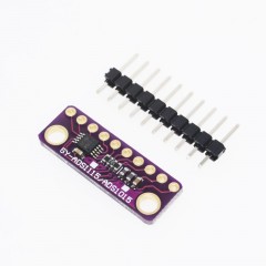
Gy-ads1115 Ads1115 16bit Adc 4ch...
-
Interfaz Tm7705 Dual Conversor...
-
Gy-ads1015 Ads1015 12bit Adc 4ch...
-
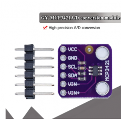
Gy-mcp3421 Adc Conversor A/d...
-
Ads1256 24bit Adc - 8ch...
-
Cjmcu-6668 Ltc1966 Adc Sigma...
-
Pcm2704 Tarjeta Sonido Usb Dac...
-
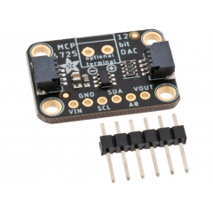
Mcp4725 Dac I2c Modulo Breakout...
-
Pcm2704 Usb Tarjeta Sonido Usb...
-
Max98357 Audio Decoder Dac Pcm...
-
Modulo Dac Xd-41b Tlc5615 10bit...
-
Mcp4725 Dac 12bit I2c Modulo...
-
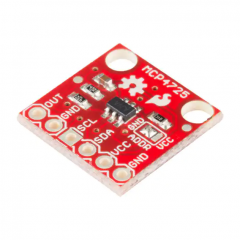
Bob-12918 Mcp4725 Dac I2c Modulo...
-
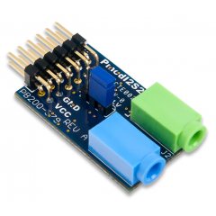
Pmod I2s2 Stereo Audio Input And...
-

Interfaz Dac 10 Bits D/a...
-
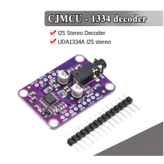
Cjmcu-1334 Dac I2s Audio...
-
Conversor Dac 12bits Mcp4725 Hat...
-
Interfaz Conversor A/d Adc0809...
-
Zy Ads1115 Ads1115 16bit Adc 4ch...
-
Interfaz Conversor A/d Hx710a...
-
Interfaz Adc A/d Sgm58031 16...
-

Mejor Precio Garantizado
En nuestra tienda encontrará los mejores precios.
-

Soporte
Por cualquier duda, puede comunicarse con nosotros.
-

Ofertas
Acceda a las mejores ofertas en nuestros productos.